From schematic to sign-off,
in one native app.
IC Studio puts schematic capture, SPICE simulation, layout, automatic place and route, DRC, LVS and parasitic extraction on one design database. Draw a circuit, generate its layout, verify it and simulate it again with the parasitics, without leaving the window or converting a single file.
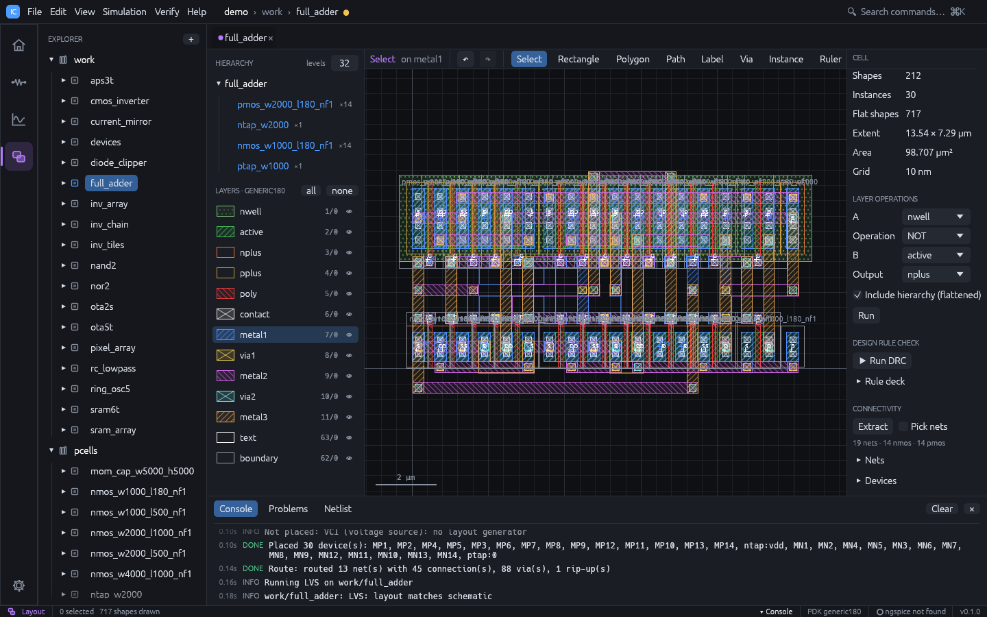
One database, the whole loop
Most open-source flows chain separate tools through netlists and GDS files. In IC Studio the schematic, the simulator and the layout share one design database, so every step knows about the others:
- Layouts are generated from schematics and routed automatically.
- Layouts are checked against schematics (LVS) with clickable differences.
- Parasitics extracted from the layout flow straight back into simulation.
What you get
Schematic and simulation
Live connectivity, operating-point annotation, DC / AC / transient analyses on a built-in simulator or ngspice, Bode plots and automatic measurements.
Automatic place and route
Transistors placed as PCells with shared diffusion, common-centroid matching and dummies; a rip-up-and-reroute maze router wires every net DRC-clean.
Hierarchical layout
Instances and arrays, level-of-detail rendering for large designs, Boolean layer operations, vias, PCells, GDSII and OASIS in and out.
Verification
Rule-deck DRC with derived layers, connectivity extraction, LVS with device merging, and sign-off runs through KLayout, Calibre or netgen.
Analysis tools
A waveform calculator, corner, parametric and Monte Carlo sweeps with specs, yield and datasheets, and run-to-run comparison of results.
Layout generators
Guard rings, via arrays, common-centroid matched placement and density fill, plus a visual DRC rule designer and Virtuoso-compatible SKILL.
Real PDKs
Start on the generic 180 nm technology, then switch to SKY130 or IHP SG13G2: layers, device recognition, models and corners from one PDK file.
Scriptable and agent-ready
Every action is a command. The ics CLI runs in CI, and the MCP server
lets an AI agent design in the window you are watching.
Try it in one minute
git clone https://github.com/geniuskey/ic-studio
cd ic-studio
cargo run --release -- --demo --cell full_adder --workspace layout
With a release installed, run
ic-studio --demo --cell full_adder --workspace layout instead. The demo project opens on an automatically placed and routed full adder. The
demo gallery walks through every example and has ready-made scripts for
presenting IC Studio live.
What is in the box
Two programs, installed together:
| Program | Purpose |
|---|---|
ic-studio | The desktop application |
ics | Command-line interface for scripting and CI |
ics mcp | The same ics program run as a Model Context Protocol server for AI agents |
All three front ends use the same core library, so a project edited in the app can be simulated, checked or exported from the command line, or driven by an agent.
Main concepts
- Project: a folder holding
ic-studio.json, the technology (tech.json) and one folder per library. Everything is human-readable JSON that diffs well in git. - Library: a named group of cells (the demo project has
workandpcells). - Cell: a design unit with up to three views: schematic, simulation (the analyses set up for the schematic) and layout.
- Workspace: the app has four workspaces, Home, Schematic, Simulation and Layout. The open cells appear as tabs shared by all workspaces; switching workspace shows the same cell in a different view.
- Technology (PDK): layers, GDS numbers, display styles, design rules and electrical coefficients. New projects start with a generic 180 nm-class technology.
How to read this guide
- New users: Installation, then the Quick tour.
- Showing IC Studio to others: the Demo gallery.
- Designing a circuit: Schematic and Simulation.
- Drawing and checking layout: Layout, Verification and Schematic-driven layout.
- Measurements, corners, Monte Carlo and layout generators: Tools.
- Using a real PDK: Technology.
- Automation: Command line and MCP server.
Keyboard shortcuts are written for Windows and Linux (Ctrl). On macOS use Cmd instead.
Press F1 in the app for the full shortcut list, or see Keyboard shortcuts.