Quick tour
This tour walks through the demo project: simulation, hierarchical layout, automatic place and route, verification and post-layout simulation. It ends by building a small circuit from scratch.
Open the demo project
cargo run --release -- --demo
Or choose Open demo project on the welcome page (File > New Demo Project). The demo
lives in memory until you save it with Ctrl+S. All cells are in the work library and
use the generic 180 nm technology.
The demo gallery describes every cell, and has scripts for presenting IC Studio to others.
The pcells library holds the PCell variants the layouts use.
1. Schematic and simulation
- In the Explorer, click
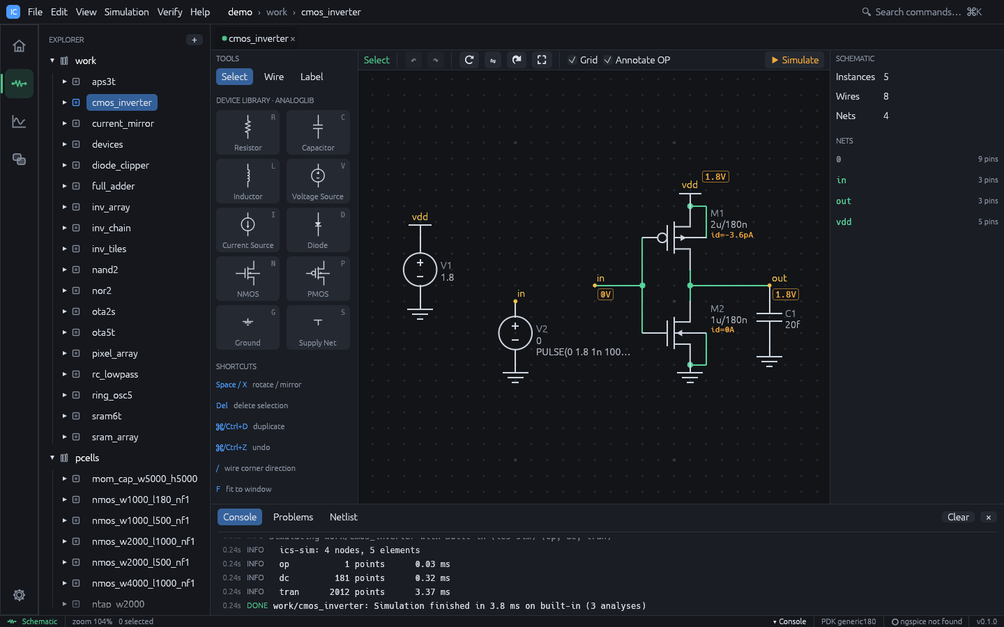
cmos_inverter. The schematic opens. - Press
F5. The Simulation workspace opens with the DC sweep and transient results. - Tick or untick signals in Signals to change the plot; read MIN / MAX / FINAL in Measurements.
- Press
Ctrl+2to go back to the schematic: node voltages and drain currents from the operating point are annotated on it.
Try rc_lowpass (AC: the f -3 dB column shows the corner frequency) and ota5t
(AC: open-loop gain and unity-gain frequency).
2. Layout and hierarchy
- Press
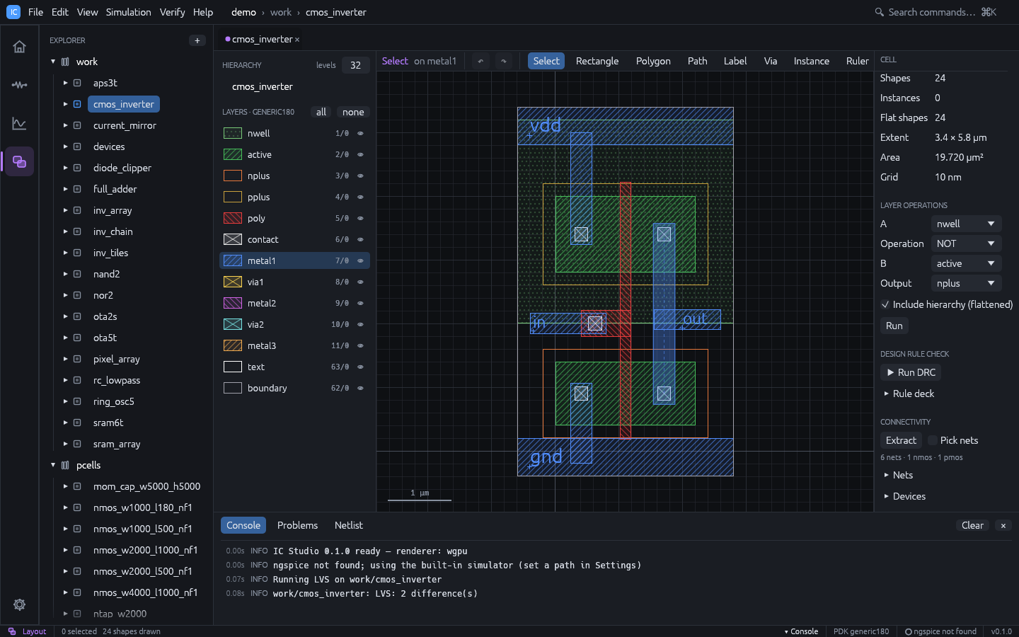
Ctrl+4withcmos_inverteropen. This layout was drawn by hand. - Open
inv_tiles(Explorer, orCtrl+Kand typeinv_tiles). Zoom withCtrl+wheel, pan with the wheel or the middle mouse button, and pressFto fit. - Press
1,2and9to change how many hierarchy levels are drawn. - Double-click an instance to open the placed cell.
3. Automatic place and route
- Open
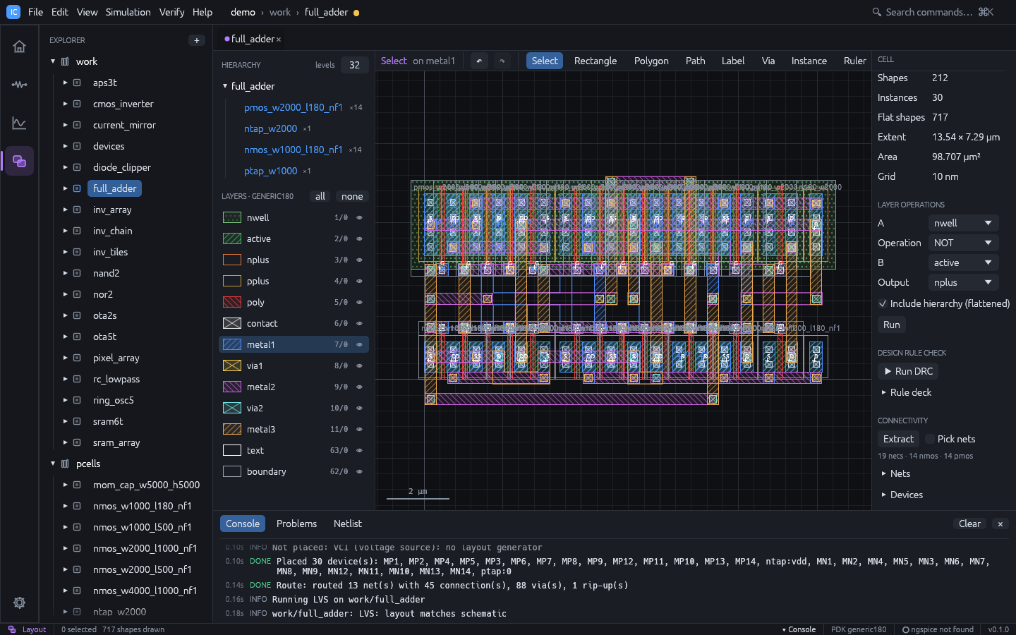
full_adderand pressCtrl+4. This layout was not drawn: it was generated from the schematic and routed automatically. - Press
Ctrl+AandDeleteto clear it. - Choose Verify > Generate Layout from Schematic. The 28 transistors are placed and flylines show the connections to make.
- Choose Verify > Route Flylines. Every net is routed on metal.
4. Verification
- Open
nand2and switch to the Layout workspace. - In the right panel, press Run DRC: no violations.
- Press Run LVS: the layout matches the schematic.
- Open
cmos_inverterand run LVS: it lists the deliberate differences. Click one to zoom to it.
5. Post-layout simulation
- Open
ring_osc5in the Simulation workspace. - Press
F5and note the oscillation period in the transient plot. - Tick Include layout parasitics and press
F5again. The console summarises the extracted capacitance and resistance. Compare the period: the added wire capacitance and resistance slow the oscillator down.
6. Build an inverter from scratch
- Press
Ctrl+N, name the cellmy_inv, keep schematic checked, and press Create. - Press
Pand click to place a PMOS, then pressNand click below it to place an NMOS. PressEsc. - Press
Wand wire the two drains together, then the two gates.Escends a wire. - Press
Sand place a supply symbol on the PMOS source; pressGand place ground on the NMOS source. Wire them. - Press
T, typeinin the Net: field and click on the gate wire; typeoutand click on the drain wire. - Add the sources: press
V, place a source, wire itsppin to the supply net and itsnpin to a ground symbol; set DC value to1.8in the inspector. Place a second source forinwith TransientPULSE(0 1.8 1n 100p 100p 2n 4n). - Press
Ctrl+3, enable Transient (step10p, stop10n) and pressF5. - Choose Verify > Generate Layout from Schematic. The two transistors are placed as PCells with well taps, and flylines show the connections to make.
- Choose Verify > Route Flylines. The router wires the nets on metal.
- Run DRC and LVS from the right panel, then save with
Ctrl+S.
See Schematic-driven layout for what the generator and the router do, and how to match devices.
7. Command line
The same project can be checked from a terminal:
ics new demo --template demo
ics sim demo ota5t
ics drc demo nand2
ics lvs demo nand2
See Command line.