Demo gallery
Every example below ships with IC Studio. Open them all with:
cargo run --release -- --demo
or choose Open demo project on the welcome page. The demo uses the generic 180 nm
technology and lives in memory until you save it with Ctrl+S. To jump straight to a cell,
add --cell <name> --workspace <schematic|simulation|layout>.
The second half of this page has step-by-step demo scripts for showing IC Studio to an audience.
Highlights
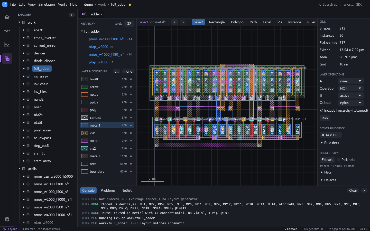
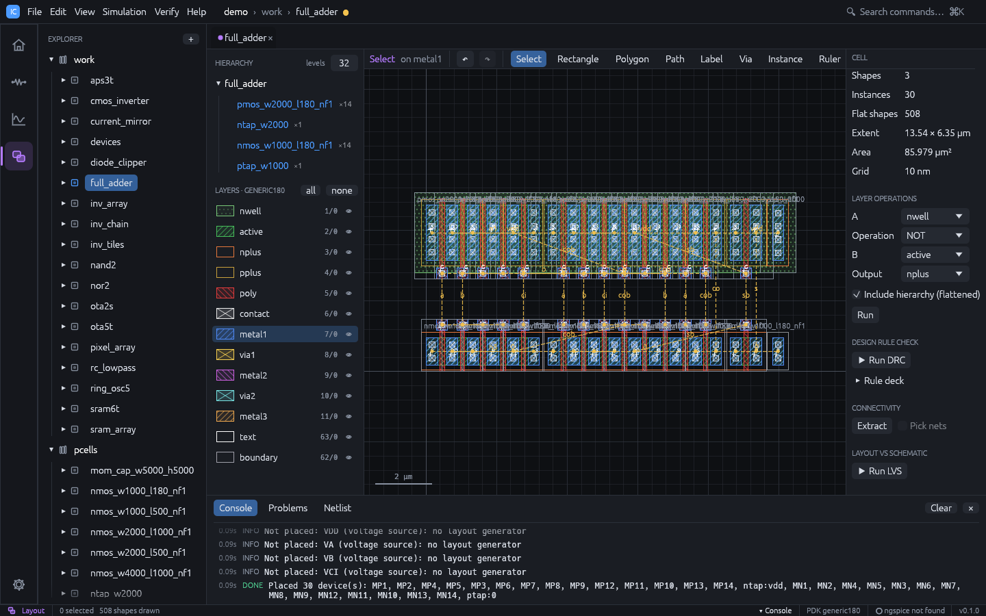
full_adder auto P&R
A 28-transistor mirror full adder whose layout was never drawn: devices placed from the schematic with shared diffusion, every net maze-routed on metal1 to metal3. DRC and LVS clean.
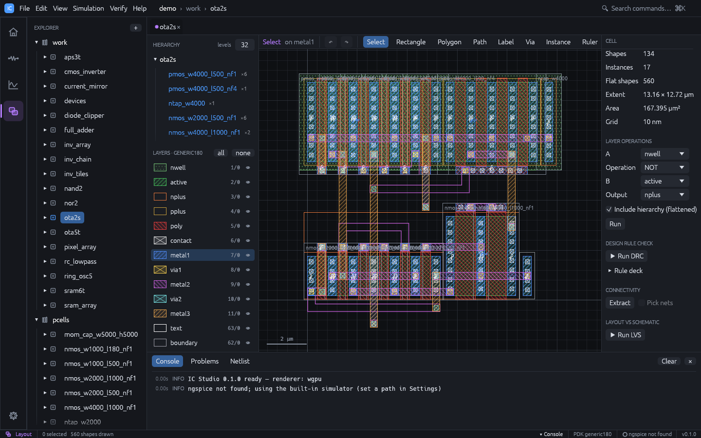
ota2s auto P&R analog
A two-stage OTA. The input pair and the current mirror are recognised, split into unit fingers, placed in common-centroid order with dummies, then routed. About 80 dB open-loop gain.
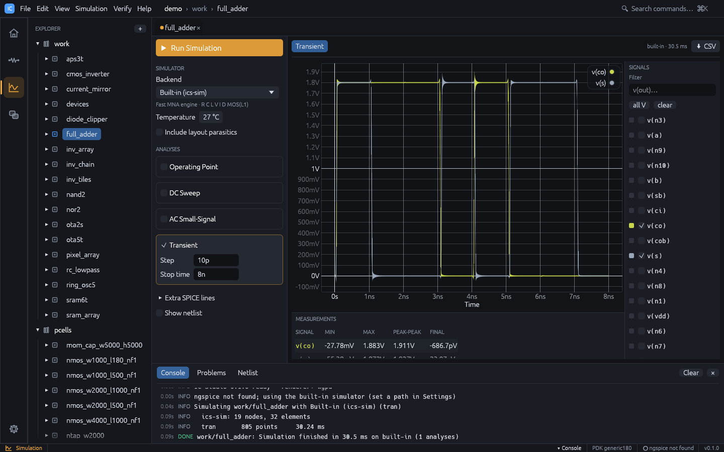
full_adder simulation
The adder’s transient run cycles through all eight input combinations; the sum and carry waveforms are the truth table.
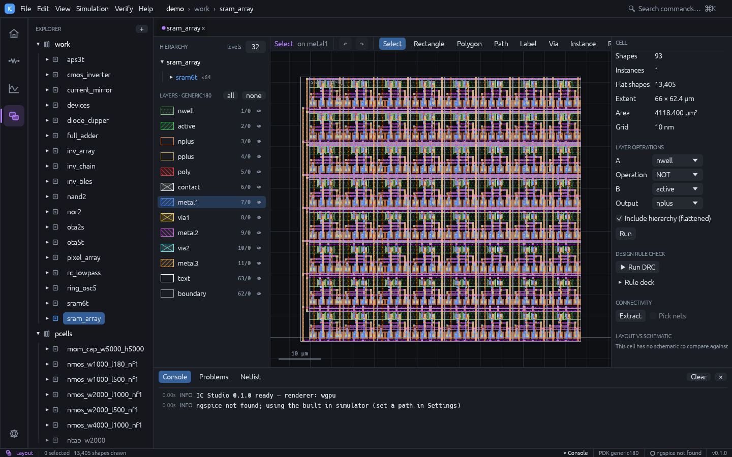
sram_array
An 8 × 8 array of the 6T bit cell sram6t, with word lines, bit lines and supply
straps. The bit cell itself is DRC and LVS clean and simulates a write and hold.
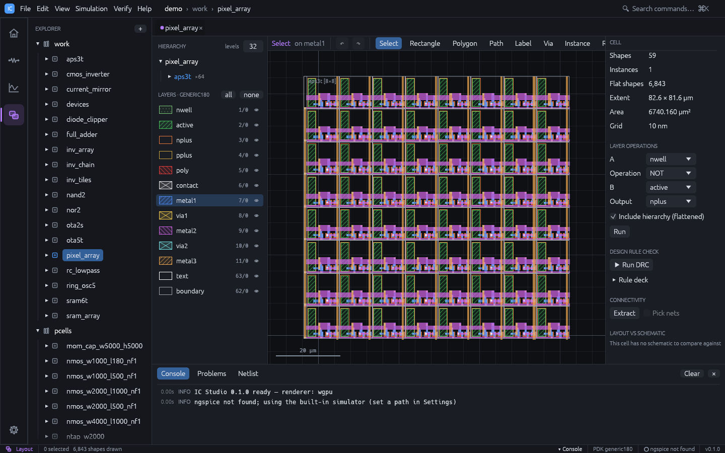
pixel_array
An 8 × 8 array of 3T image sensor pixels (aps3t: reset, source follower, row select
over an n+ / p-substrate photodiode) with labelled rows and columns.
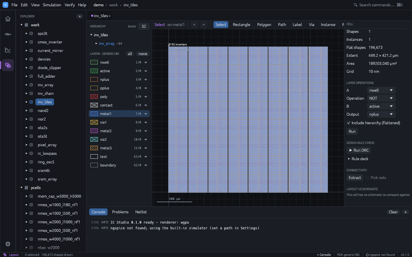
inv_tiles
8,192 inverters in two levels of arrays, about 250k flattened shapes. Level-of-detail rendering keeps pan and zoom smooth.
All demo cells
| Cell | What it shows |
|---|---|
full_adder | 28T mirror full adder, placed and routed automatically; transient over all input combinations |
ota2s | Two-stage OTA, auto P&R with common-centroid matching; about 80 dB open-loop gain in AC |
cmos_inverter | Inverter with a hand-drawn layout; LVS reports deliberate findings (PMOS W, load cap) |
rc_lowpass | RC low-pass filter (fc about 159 kHz): OP, AC and transient |
diode_clipper | Resistor and shunt diode clipper: transient and DC sweep |
nand2 | 2-input NAND: schematic plus routed PCell layout, DRC and LVS clean |
nor2 | 2-input NOR: schematic plus routed PCell layout, DRC and LVS clean |
ring_osc5 | 5-stage ring oscillator, fully routed; slows down visibly with layout parasitics |
current_mirror | NMOS current mirror with a 20 µA reference: DC sweep of the output |
ota5t | 5-transistor OTA: about 42 dB open-loop gain in AC |
sram6t | 6T SRAM bit cell, DRC and LVS clean: transient write and hold |
sram_array | 8 × 8 array of sram6t |
aps3t | 3T image sensor pixel, DRC and LVS clean: transient reset and integration |
pixel_array | 8 × 8 array of aps3t |
inv_chain | Four placed cmos_inverter instances |
inv_array | 16 × 8 array of inverters |
inv_tiles | 8 × 8 array of inv_array: 8,192 inverters, two levels of hierarchy |
devices | One instance of every PCell |
Every cell with both a schematic and a layout (full_adder, ota2s, nand2, nor2,
ring_osc5, current_mirror, ota5t, sram6t, aps3t) runs the whole flow:
simulate, open the layout, run DRC and LVS, and simulate again with parasitics.
Demo scripts
Each script is a sequence you can run in front of an audience, with the result to expect at every step. The blue boxes suggest what to say.
1. Five-minute tour
The whole loop on one circuit: schematic, simulation, automatic layout, verification and post-layout simulation.
-
Start the app on the adder’s schematic:
cargo run --release -- --demo --cell full_adder --workspace schematic -
Press
F5. The Simulation workspace opens with the transient run:a,bandcistep through all eight combinations, andsandcofollow the truth table. -
Press
Ctrl+4for the layout. Select everything withCtrl+Aand pressDelete. The layout is empty. -
Choose Verify > Generate Layout from Schematic. The 28 transistors appear as PCells in a PMOS row over an NMOS row, with well taps, and dashed flylines show every connection still to make.
-
Choose Verify > Route Flylines. The flylines are replaced by metal1 to metal3 wires and vias; the console reports the nets routed.
-
In the right panel press Run DRC (no violations), then Run LVS (the layout matches the schematic).
-
Press
Ctrl+3, tick Include layout parasitics and pressF5. The console summarises the extracted capacitance and resistance, and the waveforms now include the wiring delay.
Say: “Nothing here was drawn by hand. The layout comes from the schematic, the router makes it DRC clean, LVS proves it is the same circuit, and the parasitics go straight back into the simulation, all on one database.”
2. Auto place and route, step by step
Slower, for an audience that cares about layout. Use the adder or the OTA.
| Step | Do | Expect |
|---|---|---|
| 1 | Open full_adder in the Layout workspace | The finished, routed layout |
| 2 | Ctrl+A, Delete | An empty layout |
| 3 | Verify > Generate Layout from Schematic | Devices placed; source / drain columns shared where nets allow; flylines on |
| 4 | Move a device with the mouse | Its flylines follow it: the link to the schematic is the instance name |
| 5 | Ctrl+Z | The device goes back |
| 6 | Verify > Route Flylines | All nets routed; the console lists nets, connections, vias and rip-ups |
| 7 | Click a device in the layout, then Ctrl+2 | The same device is selected in the schematic (cross-probing) |
| 8 | Run DRC, Run LVS | No violations; layout matches schematic |
Say: “The router is a maze router with rip-up and reroute. Its grid is aligned to the device terminals, so what it draws is DRC clean by construction, and it labels the named nets so LVS can anchor them.”
3. Analog matching
Shows that the generator understands analog structure, not only connectivity.
- Open
ota2sin the Layout workspace,Ctrl+A,Delete. - Verify > Generate Layout from Schematic. The console reports the matched groups,
for example the differential pair and the mirror placed as
ABBAwith dummy fingers at both ends. - Verify > Route Flylines, then Run LVS. LVS merges the unit fingers back into the seven schematic devices and ignores the dummies.
- Press
Ctrl+3andF5. The AC plot shows about 80 dB of open-loop gain.
Say: “Differential pairs and current mirrors are detected from the schematic. They are split into unit fingers and placed in common-centroid order, the way an analog layout engineer would, and LVS still sees seven transistors.”
4. Post-layout effects
- Open
ring_osc5in the Simulation workspace and pressF5. Note the oscillation period. - Tick Include layout parasitics and press
F5again. The period gets longer: the wire capacitance and resistance extracted from the layout slow the ring down.
5. Scale
- Open
inv_tilesin the Layout workspace: 8,192 inverters. - Zoom with
Ctrl+wheel, pan with the wheel or the middle mouse button,Fto fit. - Press
1,2and9to change how many hierarchy levels are drawn, and double-click an instance to descend into it.
6. Command line and CI
The same flow without a window, from a SPICE netlist to a verified GDS. Save this as
ota.cir:
* two-stage OTA
M1 x inp tail 0 nmos w=4u l=500n
M2 o1 inn tail 0 nmos w=4u l=500n
M3 x x vdd vdd pmos w=8u l=500n
M4 o1 x vdd vdd pmos w=8u l=500n
M5 tail vb 0 0 nmos w=4u l=1u
M6 out o1 vdd vdd pmos w=16u l=500n
M7 out vb 0 0 nmos w=4u l=1u
VDD vdd 0 dc 1.8
VINP inp 0 dc 0.9 ac 1
VINN inn 0 dc 0.9
VB vb 0 dc 0.65
.ac dec 20 1k 10g
Then:
ics new demo                         # project with the demo cells
ics schematic demo my_ota ota.cir    # netlist -> schematic and simulation setup
ics route demo my_ota --place        # place, route, save
ics drc demo my_ota                  # 0 violations
ics lvs demo my_ota                  # layout matches schematic
ics sim demo my_ota --parasitics     # post-layout AC
ics gds demo my_ota -o my_ota.gds    # stream out
Every command exits non-zero on failure, so the sequence drops into a CI job as is. See Command line.
7. An AI agent designs while you watch
With the MCP server registered in an agent such as Claude Code, start the app
(cargo run --release -- --demo) and ask the agent:
In the open IC Studio project, create a cell
my_otafrom this netlist (pasteota.cir), generate its layout, route it, run DRC and LVS, then simulate AC and tell me the open-loop gain.
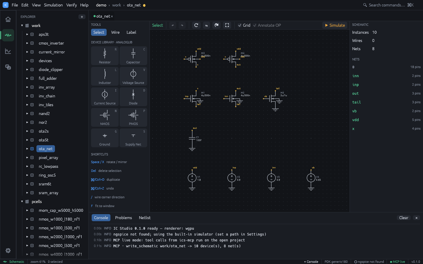
The status bar shows MCP live. The schematic appears in the window, then the placed
devices, the routed wires, the DRC and LVS results and the AC plot, each logged in the
console as MCP · <tool> .... Every layout step can be undone with Ctrl+Z.
Say: “The agent uses the same commands as the menus. It is not generating a file for you to import; it is working in your session, and you can take over at any point.”