Schematic-driven layout
IC Studio can build a layout from a schematic: it places the transistors as PCells, shows the connections still to be made as flylines, and routes them.
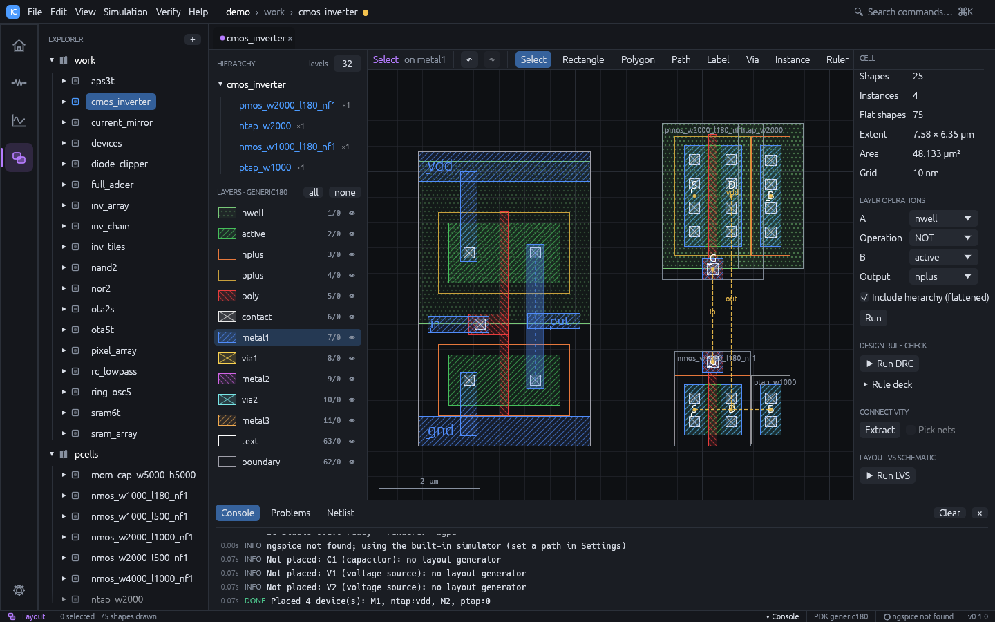
Step by step
- Draw and simulate the schematic. Give the external nets labels (
in,out, …); use the Ground and Supply symbols for the rails. - With the cell active, choose Verify > Generate Layout from Schematic. The cell gets a layout view if it has none, and the Layout workspace opens with flylines on.
- Inspect the placement. Move devices if you want; their names keep the link to the schematic.
- Choose Verify > Route Flylines to route the remaining connections.
- Add pin labels on metal for the external nets (Label tool,
L) so that LVS can anchor them. - Run DRC and LVS (see Verification), then simulate with Include layout parasitics.
Each step can be undone with Ctrl+Z. The console lists what was placed, skipped,
matched and routed.
Demo: auto P&R
The demo cells full_adder (28 transistors) and ota2s (two-stage OTA with a
common-centroid input pair and mirror) have layouts made only by this flow. Clear one
(Ctrl+A, Delete) and run the two commands above to watch it happen. The
demo gallery has a complete script.
Placement
- Each NMOS and PMOS becomes a PCell instance named after the schematic device (
M1). W and L come from the device’swandlparameters;mmultiplies the device. Devices wider than 5 µm are split into fingers. With a PDK, the schematic model selects the PCell’s device (and its marker layers, such aslvtnfor a low-Vt model). - PMOS devices form a row above the NMOS row, gates facing the channel between the rows.
- Neighbouring devices of the same type and width that share a source / drain net are abutted with shared diffusion.
- Wells and implants are merged across each row, and each row ends with a bulk tap
(
ntapin the PMOS row,ptapin the NMOS row) on the row’s bulk net. - Devices already in the layout (by name) are left alone, so you can generate again after adding devices to the schematic.
- Devices without a layout generator (R, C, L, diodes, sources) are skipped and listed in the console.
Matched devices
Differential pairs and current mirrors are detected automatically:
- Differential pair: two devices of the same type, W, L and m with a common source net that is not a rail, and different gates and drains.
- Current mirror: devices of the same type and L with a common gate and source, where the gate is tied to one device’s drain.
You can also group devices explicitly by giving them the same match parameter, or opt a
device out with match=none. The inspector shows only the standard parameters, so add
match (and match_rows) to the device’s params in the cell’s schematic.json:
"params": { "model": "nmos", "w": "4u", "l": "500n", "m": "1", "match": "pair1" }
A matched group is split into equal unit fingers named <device>.<k> (for example
M1.1, M1.2), placed in common-centroid order (ABBA). Groups of 8 units or more, or
groups with match_rows=2, use two cross-coupled rows (ABBA / BAAB); match_rows=1
forces a single row. Each unit row is closed by dummy fingers at both ends whose gates
are tied to bulk; LVS ignores them because they are always off.
The console reports each group, for example A, B: matched as ABBA (A = M1, B = M2), or
why it could not be matched.
Flylines
The Flylines checkbox in the layout toolbar draws a dashed line, labelled with the net name, for every schematic connection that is not yet made in the layout. They update after every edit, so you can route by hand and watch them disappear.
Router
Route Flylines runs a maze router (A* search) over the routing metal layers above poly (metal1, metal2 and metal3 in the generic technology):
- The routing grid is aligned to the device terminals; wires have one width that fits a via, with DRC spacing between tracks.
- Existing geometry is avoided. Short nets are routed first; nets that block each other are ripped up and rerouted.
- Metal1 is expensive and each higher layer has a preferred direction, so long runs move to upper metals.
Every named schematic net (labels and supplies; the ground symbol becomes gnd) that is
fully connected after routing gets a text label at one of its terminals, unless the top
cell already has a label of that name. The label goes on the first metal, or on the layer
the PDK names for its net labels ([[pin_label]], e.g. Metal1.text in SG13G2), so
external LVS decks see the layout’s ports with their schematic names.
The console summary gives the routed nets, connections, vias and rip-ups. Nets that could not be routed stay as flylines with a reason (terminals not on conducting geometry, or pieces not reached). Finish them by hand and route again.
Cross-probing
Select a device in the schematic and switch to the layout: the instances with the same name (including its unit fingers) are selected, and the other way round.
From the command line or an agent
ics route myproj nand2 --place # place missing devices, route, save; exit 1 if nets remain
The MCP server offers generate_layout, flylines and route (see MCP server).