Verification: DRC, extraction and LVS
The verification tools are in the Verify menu and in the right panel of the Layout workspace. They run in the background on the flattened layout of the active cell; while one runs, the panel shows its progress and a Cancel button. After you edit the layout, the panel notes that results are out of date.
Design rule check (DRC)
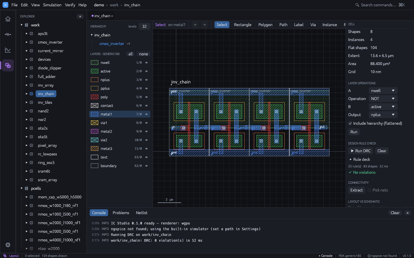
- Open the cell’s layout.
- Press Run DRC in the Design Rule Check section (or Verify > Run DRC).
- The result is either No violations or a list grouped by rule, with a count per rule. Markers are drawn on the canvas.
- Expand a rule to see its description and the violation locations; click one to zoom to it.
- Clear removes the results and markers.
The rules come from the technology’s deck. Expand Rule deck to view and edit it in
place: Run DRC uses the edited text right away, Save to technology stores it in
the project’s tech.json, and Reset replaces it with the deck derived from the
technology’s layer and via rules. Syntax errors are listed by line. See
Technology for the deck syntax. Rule Designer… (also
Tools > DRC Rule Designer) edits the deck as forms and self-tests every rule on
generated patterns; see DRC Rule Designer.
A layer that fails a density rule can be filled with Tools > Dummy Fill (see
Dummy Fill).
DRC checks Manhattan geometry; other shapes are skipped and counted. Distances between corners are Euclidean.
Live DRC
The Live DRC checkbox in the layout toolbar re-checks the deck around every edit in the
background and draws the violations as dashed boxes as they appear; hover one to see its
rule. Quick Fix (Ctrl+.) on a violation offers candidate edits of top-level shapes
(reshape, move or add), each checked with DRC first and marked clean or with the number
of new violations it causes; it turns live DRC on when it is off. Fix All Violations
(command palette) applies fixes until none helps any more, as one undoable step. Geometry
inside placed cells is not changed.
Connectivity extraction
- Press Extract in the Connectivity section (or Verify > Extract Nets).
- The summary shows the number of nets and NMOS / PMOS transistors.
- Click a net in Nets to highlight it. Check Pick nets and click a shape on the canvas to highlight the net it belongs to.
- Devices lists each transistor with W, L and its terminal nets; click one to zoom to its gate.
Tools > Net Browser lists the extracted nets in a sortable table with their layers, area, transistor terminals and wire capacitance; click one to highlight it and zoom to it (see Net Browser).
How the extractor works:
- Conducting layers are the layers joined by vias. Diffusion is
activeminuspoly. - A transistor is
polyoveractive. It is PMOS when it is insidepplus(or insidenwellwhen there is no implant). L is measured across the gate; W is area / L. - Net names come from labels in the top cell on conducting layers. Unnamed nets are called
netN. - Warnings report labels not on conducting geometry, two labels shorted together, and a label on several unconnected pieces.
Layout versus schematic (LVS)
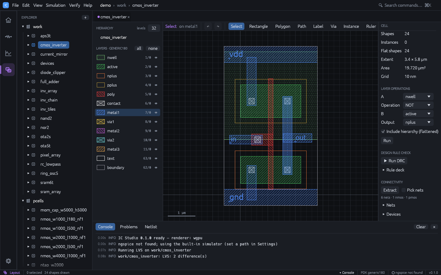
-
The cell needs both a schematic and a layout. Device names do not have to match, but labels on the layout’s pins (
in,out,vdd, …) help: equal net names anchor the comparison. -
Press Run LVS (or Verify > Run LVS).
-
The result is Layout matches schematic or a list of differences, each tagged:
[missing]: a schematic device not found in the layout,[extra]: a layout device not in the schematic,[param]: W or L differ by more than 1 %,[net]: a net whose connections differ.
Click a difference with a location to zoom to it.
Comparison rules:
- Only MOS transistors are compared. Voltage and current sources are ignored; other schematic devices (R, C, diodes) are reported as not extracted.
- Parallel devices with the same terminals and L are merged and their widths summed, so
multi-finger layouts match single schematic devices; the schematic
mmultiplies W. - Bulk terminals are ignored.
- Devices that are always off (gate tied to bulk), such as dummy fingers, are dropped.
- Net names are compared case-insensitively;
0,gndandvssare treated as the same.
The demo cell cmos_inverter deliberately has LVS findings (a PMOS width and the load
capacitor); nand2, nor2, ring_osc5, current_mirror, ota5t, sram6t, aps3t, full_adder and ota2s are clean.
Sign-off with external tools
The built-in checks are fast and good for iterating. For sign-off, a technology can list runsets that run a foundry or PDK deck in an external tool:
| Tool | Checks | Deck |
|---|---|---|
| KLayout | DRC, LVS | KLayout .drc / .lvs script |
| Siemens Calibre | DRC, LVS | SVRF rule file |
| netgen | LVS | netgen setup file (compares IC Studio’s extraction with the schematic) |
| built-in | DRC | IC Studio or SVRF deck file, run on the built-in engine |
In the Layout workspace, the Sign-off section appears when the technology has
runsets. Pick a Runset and press Run <cell>.gds in a new temporary folder, plus
the schematic as a .subckt for LVS, runs the tool there and reads its report:
- DRC violations appear as markers on the canvas, like the built-in DRC. Violations the tool reports inside sub-cells keep sub-cell coordinates and name the cell.
- LVS shows whether the layout matches and the tool’s messages.
- The folder (shown under the result) keeps the inputs, reports and the tool’s log.
How each tool is called:
- KLayout:
klayout -b -r DECK -rd input=CELL.gds -rd topcell=CELL -rd report=FILE, plus-rd schematic=CELL_sch.cirfor LVS and the runset’svars. The variable names can be changed withklayout = { input = "...", topcell = "...", report = "...", schematic = "..." }. - Calibre: a control file sets
LAYOUT PATH,LAYOUT PRIMARY,LAYOUT SYSTEM, the ASCII results database (DRC) orSOURCE PATH/LVS REPORT(LVS), adds#DEFINEfor each var andINCLUDEs the deck. The deck itself must not set these statements. Thencalibre -drc -hierorcalibre -lvs -hier -spice. - netgen:
netgen -batch lvs "CELL_lay.cir CELL" "CELL_sch.cir CELL" SETUP REPORT.
The schematic netlist leaves out the element letters in the runset’s skip (default
V and I) and names the ground net ground (default gnd). Executables are found on
the usual install paths and PATH; set ICS_KLAYOUT, ICS_CALIBRE or ICS_NETGEN to
override them.
Runsets come from a PDK file ([[signoff]]) or the signoff
array in tech.json:
"signoff": [
  {"name": "KLayout DRC", "tool": "klayout", "check": "drc", "deck": "/pdk/rules.drc",
   "vars": {"feol": "true"}},
  {"name": "Calibre LVS", "tool": "calibre", "check": "lvs", "deck": "/pdk/calibre.lvs",
   "skip": ["V", "I", "C"]}
]
From the command line
ics drc myproj nand2 [--deck rules.drc]   # exit code 1 on violations
ics extract myproj nand2                  # extracted SPICE netlist
ics lvs myproj nand2                      # exit code 1 on differences
ics signoff myproj nand2                  # list the sign-off runsets
ics signoff myproj nand2 "KLayout DRC"    # run one; exit code 1 on violations / mismatch
These exit codes make the checks usable in CI. See Command line.