Schematic editor
Open a cell’s schematic view (or press Ctrl+2 with a cell open) to edit it.
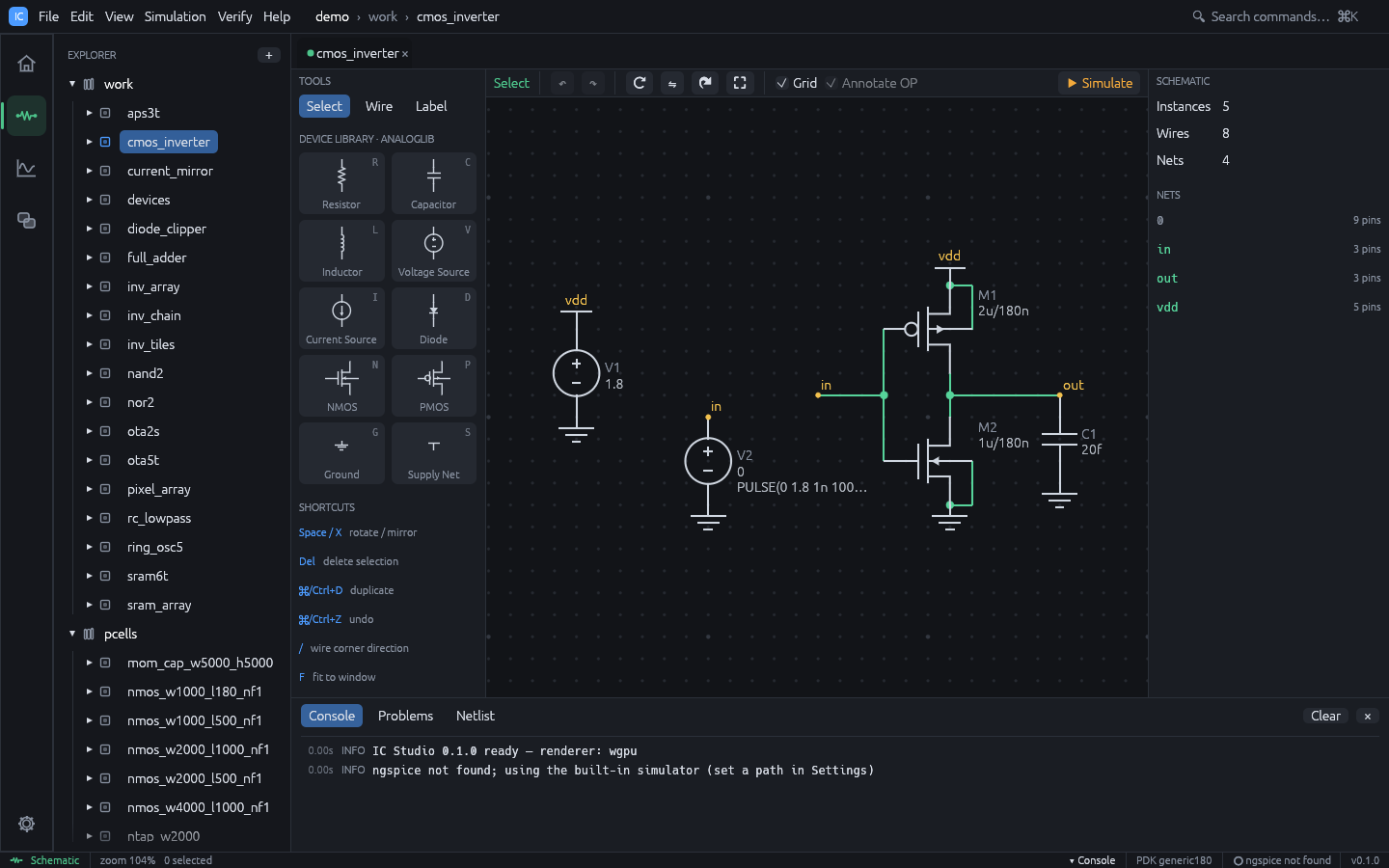
- Left panel: Tools (Select, Wire, Label), the Device Library with one tile per primitive and its shortcut letter, and a short shortcut reminder.
- Toolbar: the current tool, undo / redo, rotate, mirror, duplicate, fit, the Grid
and Annotate OP checkboxes, and Simulate (
F5). - Right panel: the property inspector.
Schematic coordinates are integer grid points. Keys act on the canvas only while the mouse is over it and no text field has focus.
Devices
| Key | Device | Name prefix | Pins | Default parameters |
|---|---|---|---|---|
R | Resistor | R | p, n | r=1k |
C | Capacitor | C | p, n | c=1p |
L | Inductor | L | p, n | l=1n |
V | Voltage Source | V | p, n | dc=1 |
I | Current Source | I | p, n | dc=1m |
D | Diode | D | a, k | model=dmod |
N | NMOS | M | d, g, s, b | model=nmos w=1u l=180n m=1 |
P | PMOS | M | d, g, s, b | model=pmos w=2u l=180n m=1 |
G | Ground | GND | gnd | (net 0) |
S | Supply Net | VDD | net | net=vdd |
Placing a device
- Press the device key (for example
N) or click its tile in the Device Library. - A ghost follows the cursor. Press
Spaceto rotate orXto mirror it before placing. - Click to place. The device snaps to the grid, gets the next free name (
M1,M2, …) and is selected. The tool stays active, so further clicks place more copies. - Press
Escor right-click to return to Select.
Wires
- Press
W(or choose Wire). - Click the start point, usually a pin.
- Click the next point. Each click adds an L-shaped pair of segments, horizontal first;
press
/to bend vertical first. - The wire ends automatically when a click lands on a pin, a wire end or the interior of
another wire. Otherwise keep clicking, and end with double-click, right-click or
Esc.
Connections are live: pins that are not connected are drawn as small squares, and a junction dot appears where three or more connections meet. Hovering or selecting a wire highlights its whole net.
Net labels and net names
- Press
T(or choose Label). A Net: field appears in the left panel (defaultnet1). - Type the name and click on a pin or wire to attach the label. Labels connect only at their exact grid point.
- A trailing number is incremented after each placement (
net1,net2, …), which is handy for buses of labels.
Labels with the same name are the same net, so labels connect parts of a schematic
without wires. Net names are chosen in this order: the Ground symbol (net 0), the
Supply Net symbol’s net parameter (blank means vdd), net labels, then automatic
names (net1, net2, …).
Notes:
- Only the Ground symbol makes net
0. A label calledgndis an ordinary net. - A Supply Net symbol only names a net. Place a voltage source on it to power it.
- Two different names on one net produce the warning “Net names ‘a’ and ‘b’ are shorted together”.
Selecting and editing
| Action | How |
|---|---|
| Select one object | Click it (labels take priority over wires, wires over devices) |
| Add or remove from selection | Shift+click or Ctrl+click |
| Box select | Drag on empty space (selects objects fully inside; Shift adds) |
| Select all | Ctrl+A |
| Move | Drag a selected object; attached wires stretch with moved pins |
| Rotate / mirror | Space / X, or the toolbar buttons |
| Duplicate | Ctrl+D (copies offset by two grid points, renamed) |
| Delete | Del or Backspace |
| Undo / redo | Ctrl+Z / Ctrl+Shift+Z or Ctrl+Y |
| Fit to window | F |
| Cancel | Esc cancels a wire, then returns to Select, then clears the selection |
Property inspector
Select a single device to edit it in the right panel. Values are SPICE strings typed as
they would appear in a netlist, with SPICE scale suffixes: 10k, 2.2p, 180n, 1meg.
- Name: the instance name. It must be unique; it also ties the device to its layout instance.
- Device fields: Resistance, Capacitance, Inductance / L, Model, Width, Multiplier, Net name (supply).
- Sources: DC value, AC magnitude (for AC analysis, e.g.
1) and Transient (e.g.PULSE(0 1 0 1n 1n 5n 10n);SIN(...)andPWL(...)also work). - Orientation and Position, and a Connections list showing the net on each pin.
With nothing selected, the inspector shows statistics (instances, wires, nets), the list of nets with their pin counts, and any Warnings (unconnected pins, duplicate names, shorted net names).
The Problems tab of the bottom panel runs the schematic checker on the active cell as you edit: missing ground, bad or duplicate names, missing or invalid values, shorted devices, voltage-source loops, floating nets, dangling wires and more. Click a finding to select its devices. Tools > Check Schematic runs the check on demand, and File > Check and Save saves only when there are no errors. See Check Schematic for every check.
Netlist
The Netlist tab of the bottom panel shows the SPICE deck of the active cell, updated as you edit. Export it with File > Export > SPICE netlist…. The netlister writes:
R1 p n value,C...,L...V1 p n DC <dc> [AC <ac>] [<tran>], likewise for current sourcesD1 a k dmodM1 d g s b <model> w=... l=... [m=...]; an unconnected bulk pin is tied to the source- default level-1 models
nmos,pmosanddmodwhen they are used. With a PDK model library, MOS models map to the PDK devices (subcircuit devices get anXprefix) and the library is loaded at the chosen corner.
Operating point annotation
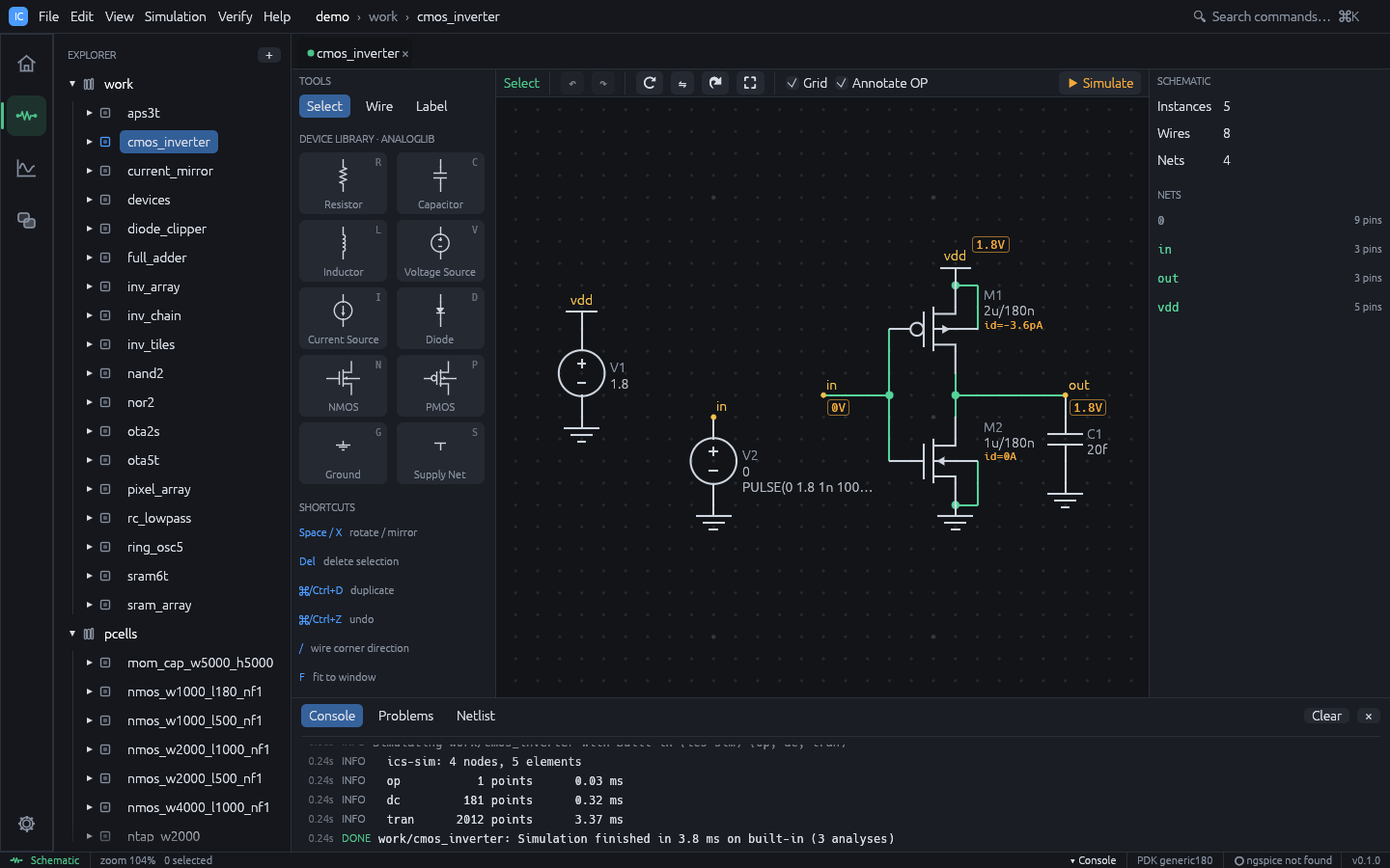
After an operating point simulation, Annotate OP (on by default) shows each node
voltage as a tag on the schematic and the current id=... under each transistor and
diode.
Cross-probing
When a cell has both a schematic and a layout, selecting devices in one editor selects the
devices with the same names in the other. Unit fingers of a matched device (M1.1,
M1.2, …) map back to M1.