Getting Started
This page walks through everything klayout-draw-mcp can do, as a sequence of prompts you might type to an AI assistant (Claude Code or Claude Desktop) with the server connected. Follow it top to bottom and you will have created, edited, inspected, DRC-checked, and placed-and-routed a layout — the whole tool set on one page.
Setup
Install and connect the server first — see Installation & Setup.
All coordinates are in micrometers; the default database grid is dbu = 0.001 (1 nm).
The screenshots are the actual rendered output of each step.
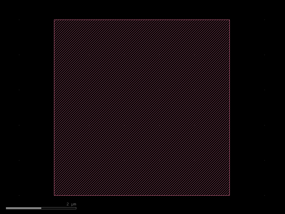
1. Your first shape
"Draw a 5×5 µm box on layer 1, save it to out.gds and open it."
The assistant calls new_layout() → add_box(1, 0, 0, 5, 5) → save_gds("out.gds", open_after=True).
2. Add to and edit a layout
"Add a 3 µm box on layer 2 in the top-right corner and label it 'edit'."
add_box(2, 5, 5, 8, 8) → add_label(63, 6.5, 6.5, "edit") → save_gds(...).
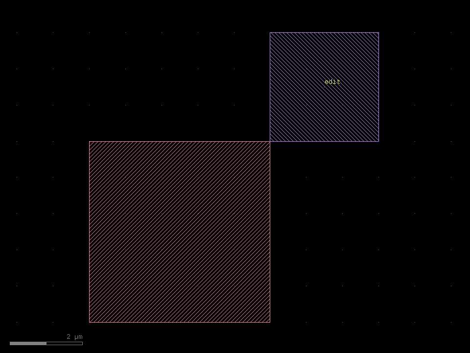
To edit a file from disk instead of the in-memory layout, start with
load_gds("out.gds") and keep adding shapes the same way.
3. Build a real cell
"Draw a CMOS inverter: a PMOS over an NMOS sharing one poly gate, with Vdd/Vss rails."
The drawing tools handle the boxes; for anything more involved the assistant uses
run_script with the full klayout.db API.
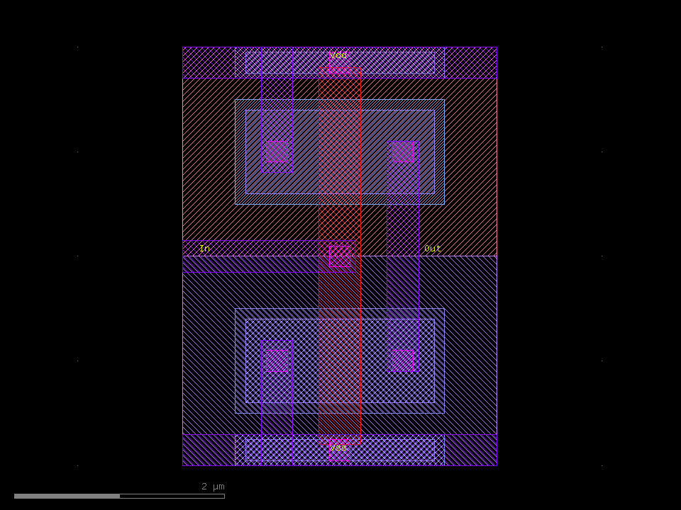
See the Examples gallery for the full source of this and other cells.
4. Hierarchy and arrays
"Make a 1 µm 4T CIS image-sensor pixel and tile it as a 2×2 array."
create_cell("PIXEL") builds the unit cell, then place_cell("PIXEL", …, nx=2, ny=2, dx=1, dy=1)
tiles it — exactly how a sensor array repeats.
![]()
5. Open and inspect an existing GDS
"Load chip.gds and tell me what's on each layer."
load_gds("chip.gds") → inspect_gds():
top_cell='CIS_APS', dbu=0.001 um, cells=2
bbox: (0,0;2,2) um
cells: ['APS_PIXEL', 'CIS_APS']

layer       shapes    area[um^2]   bbox[um]
2/0              4        4.0000   (0,0)-(2,2)
3/0             16        2.4192   (0.08,0.06)-(1.94,1.94)
6/0             16        0.3936   (0.5,0.16)-(1.97,1.82)
9/0             12        0.3200   (0.62,0.06)-(1.95,1.94)
10/0             4        1.8000   (0.05,0.05)-(1.55,1.95)
6. Design-rule checks
"Check that M1 spacing is ≥ 0.15 µm and that OD never overlaps POLY, and report where."
drc_check([...]) returns PASS/FAIL with violation locations:
DRC: 2 rules, 2 failing
spacing 3/0 >= 0.15um: FAIL (8 violations)  at (0.550,0.692), (1.010,0.500), (1.820,1.000), ...
forbidden overlap 3/0 & 6/0: FAIL (20 regions, 0.2784 um^2)  at (0.820,0.200), (1.820,0.200), ...
Because each violation has a location, the assistant can move the offending shape and re-run — a closed correction loop. See Editing & DRC.
7. Place and route
"Place six cells in two rows and connect them with M1, routing around the cells."
place_cell lays the cells down; add_wire / add_via draw routes, and for automatic
obstacle-aware routing the assistant runs a maze router in run_script:
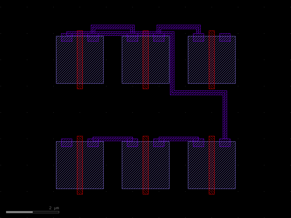
The full technique stack — row placement, vias, and the maze router — is in Placement & Routing.
Where to go next
- Examples — full source for each layout above
- Editing & DRC — loading, inspection and design-rule checks
- Placement & Routing — the P&R building blocks and recipes
- Home — the complete tool reference