Examples
Self-contained scripts live in examples/.
Each one builds a layout with the standalone klayout.db module and writes a GDS:
You can also paste the body of a script's build() function into the run_script
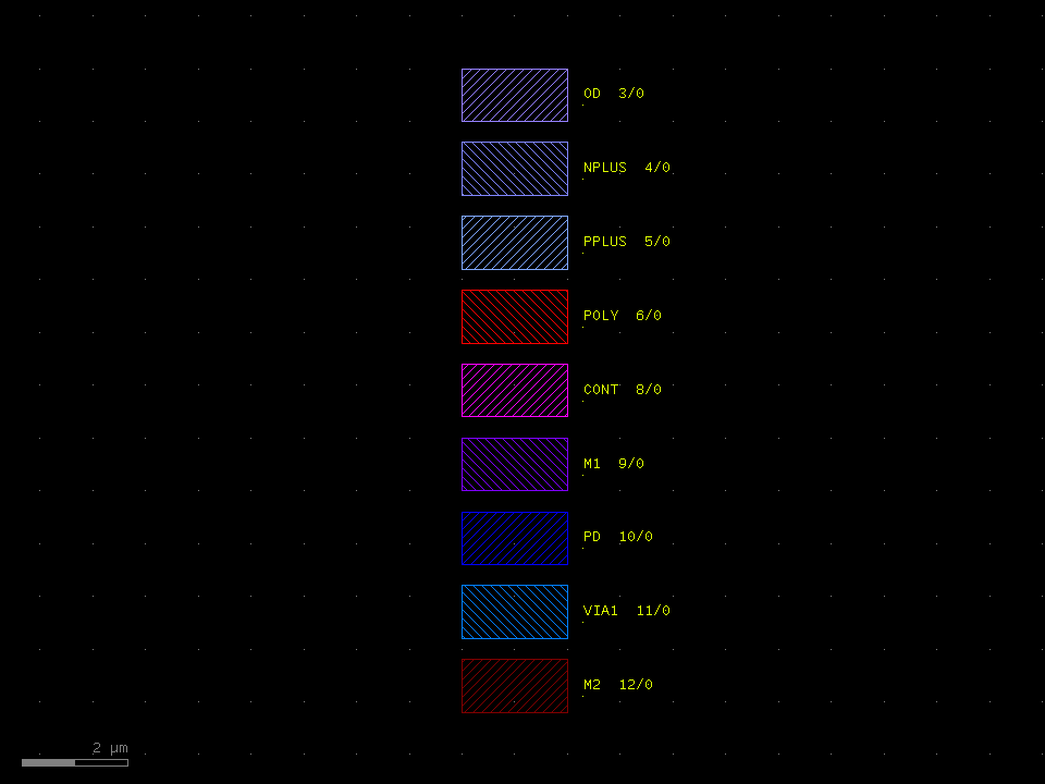
tool. All examples share one layer map (OD 3/0, POLY 6/0, NPLUS 4/0,
PPLUS 5/0, METAL1 9/0, NWELL 1/0, PWELL 2/0, CONT 8/0, TEXT 63/0, …).
The screenshots below are rendered headlessly with klayout.lay by
scripts/render_examples.py,
the same way the documentation builds them in CI.
All examples share one layer map; this is how KLayout colours those layers:
Basic shapes
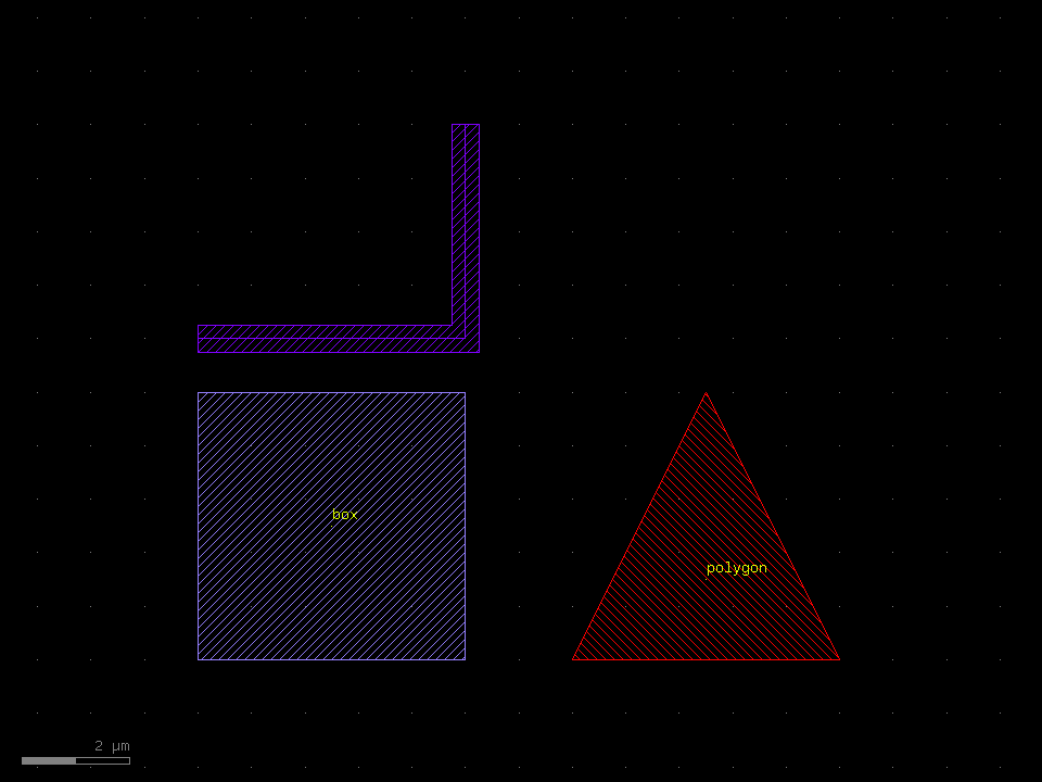
The four primitives — box, path, polygon and label — on a few layers. The place to start if you just want to see geometry come out.
"""Basic shapes sample for klayout-draw-mcp.

Shows the four primitives (box, path, polygon, label) on a few layers.

Run standalone:
    uv run python examples/basic_shapes.py [out.gds]

Or paste the body of ``build()`` into the ``run_script`` MCP tool (``db`` is
injected there; ``ly``/``top`` map to ``session.layout``/``session.top``).
"""

from __future__ import annotations

import klayout.db as db

# Shared layer map used across the examples: name -> (layer, datatype)
LAYERS = {
    "OD": (3, 0),     # active / diffusion
    "POLY": (6, 0),   # gate poly
    "M1": (9, 0),     # metal 1
    "TEXT": (63, 0),  # labels
}


def build() -> db.Layout:
    ly = db.Layout()
    ly.dbu = 0.001  # 1 nm grid
    top = ly.create_cell("BASIC")

    def lay(name: str) -> int:
        return ly.layer(*LAYERS[name])

    def box(name, x1, y1, x2, y2):
        top.shapes(lay(name)).insert(db.DBox(x1, y1, x2, y2))

    def path(name, pts, width):
        top.shapes(lay(name)).insert(db.DPath([db.DPoint(*p) for p in pts], width))

    def polygon(name, pts):
        top.shapes(lay(name)).insert(db.DPolygon([db.DPoint(*p) for p in pts]))

    def label(name, x, y, text):
        top.shapes(lay(name)).insert(db.DText(text, db.DTrans(db.DVector(x, y))))

    # a rectangle
    box("OD", 0.0, 0.0, 5.0, 5.0)

    # a 0.5 um wide L-shaped path
    path("M1", [(0.0, 6.0), (5.0, 6.0), (5.0, 10.0)], 0.5)

    # a triangle polygon
    polygon("POLY", [(7.0, 0.0), (12.0, 0.0), (9.5, 5.0)])

    # a couple of labels
    label("TEXT", 2.5, 2.5, "box")
    label("TEXT", 9.5, 1.5, "polygon")

    return ly


if __name__ == "__main__":
    import sys

    out = sys.argv[1] if len(sys.argv) > 1 else "basic_shapes.gds"
    layout = build()
    layout.write(out)
    print(f"wrote {out}  bbox={layout.top_cell().dbbox().to_s()} um")
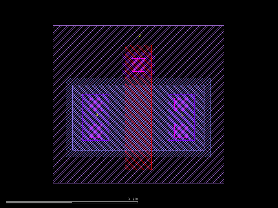
NMOS transistor
A single planar n-channel MOSFET (W = 1 µm, L = 0.4 µm): active diffusion, a poly gate crossing the channel, n+ source/drain implant, and contacts plus metal-1 pads for source (S), gate (G) and drain (D).
"""Single NMOS transistor sample for klayout-draw-mcp.

A planar n-channel MOSFET (W = 1 um, L = 0.4 um): active diffusion, a poly
gate crossing the channel, n+ source/drain implant, contacts and metal-1 pads
for source (S), gate (G) and drain (D).

Run standalone:
    uv run python examples/nmos_transistor.py [out.gds]

Or paste the body of ``build()`` into the ``run_script`` MCP tool.
"""

from __future__ import annotations

import klayout.db as db

# Shared layer map: name -> (layer, datatype)
LAYERS = {
    "PWELL": (2, 0),
    "OD": (3, 0),     # active / diffusion
    "NPLUS": (4, 0),  # n+ source/drain implant
    "POLY": (6, 0),   # gate poly
    "CONT": (8, 0),   # contact
    "M1": (9, 0),     # metal 1
    "TEXT": (63, 0),  # labels
}


def build() -> db.Layout:
    ly = db.Layout()
    ly.dbu = 0.001
    top = ly.create_cell("NMOS")

    def lay(name: str) -> int:
        return ly.layer(*LAYERS[name])

    def box(name, x1, y1, x2, y2):
        top.shapes(lay(name)).insert(db.DBox(x1, y1, x2, y2))

    def label(name, x, y, text):
        top.shapes(lay(name)).insert(db.DText(text, db.DTrans(db.DVector(x, y))))

    # well + active + implant
    box("PWELL", -0.3, -0.5, 2.3, 1.9)
    box("NPLUS", -0.1, -0.1, 2.1, 1.1)
    box("OD", 0.0, 0.0, 2.0, 1.0)          # W = 1.0 um

    # poly gate crossing the channel (L = 0.4 um), extended up for a contact
    box("POLY", 0.8, -0.3, 1.2, 1.6)

    # contacts: two on source, two on drain, one on the gate landing
    for cy in (0.3, 0.7):
        box("CONT", 0.25, cy - 0.1, 0.45, cy + 0.1)   # source
        box("CONT", 1.55, cy - 0.1, 1.75, cy + 0.1)   # drain
    box("CONT", 0.9, 1.2, 1.1, 1.4)                    # gate

    # metal-1 pads
    box("M1", 0.15, 0.15, 0.55, 0.85)   # S
    box("M1", 1.45, 0.15, 1.85, 0.85)   # D
    box("M1", 0.75, 1.1, 1.25, 1.5)     # G

    label("TEXT", 0.35, 0.5, "S")
    label("TEXT", 1.0, 1.7, "G")
    label("TEXT", 1.65, 0.5, "D")

    return ly


if __name__ == "__main__":
    import sys

    out = sys.argv[1] if len(sys.argv) > 1 else "nmos.gds"
    layout = build()
    layout.write(out)
    print(f"wrote {out}  bbox={layout.top_cell().dbbox().to_s()} um")
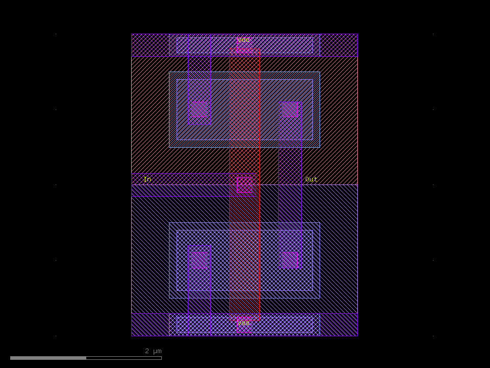
CMOS inverter
A pull-up PMOS (in an n-well, top) over a pull-down NMOS (in the p-well, bottom), sharing one poly gate (the input, in red). The two drains are tied together on metal-1 (the output). Vdd rails the top, Vss the bottom, with well ties on each.
"""CMOS inverter sample for klayout-draw-mcp.

A pull-up PMOS (in an n-well, top) over a pull-down NMOS (in the p-well,
bottom) sharing one poly gate (the input). The two drains are tied together
on metal-1 (the output). Power rails: Vdd on top, Vss on the bottom, plus
well ties.

Run standalone:
    uv run python examples/cmos_inverter.py [out.gds]

Or paste the body of ``build()`` into the ``run_script`` MCP tool.
"""

from __future__ import annotations

import klayout.db as db

# Shared layer map: name -> (layer, datatype)
LAYERS = {
    "NWELL": (1, 0),
    "PWELL": (2, 0),
    "OD": (3, 0),     # active / diffusion
    "NPLUS": (4, 0),  # n+ implant (nmos s/d, n-well tie)
    "PPLUS": (5, 0),  # p+ implant (pmos s/d, p-well tie)
    "POLY": (6, 0),   # gate poly
    "CONT": (8, 0),
    "M1": (9, 0),
    "TEXT": (63, 0),
}


def build() -> db.Layout:
    ly = db.Layout()
    ly.dbu = 0.001
    top = ly.create_cell("INVERTER")

    def lay(name: str) -> int:
        return ly.layer(*LAYERS[name])

    def box(name, x1, y1, x2, y2):
        top.shapes(lay(name)).insert(db.DBox(x1, y1, x2, y2))

    def label(name, x, y, text):
        top.shapes(lay(name)).insert(db.DText(text, db.DTrans(db.DVector(x, y))))

    # wells (p-well bottom, n-well top)
    box("PWELL", 0.0, 0.0, 3.0, 2.0)
    box("NWELL", 0.0, 2.0, 3.0, 4.0)

    # transistor active areas
    box("OD", 0.6, 0.6, 2.4, 1.4)    # NMOS
    box("OD", 0.6, 2.6, 2.4, 3.4)    # PMOS
    box("NPLUS", 0.5, 0.5, 2.5, 1.5)
    box("PPLUS", 0.5, 2.5, 2.5, 3.5)

    # well ties along the rails (p+ tie in p-well, n+ tie in n-well)
    box("OD", 0.6, 0.05, 2.4, 0.25)
    box("PPLUS", 0.5, 0.0, 2.5, 0.3)
    box("OD", 0.6, 3.75, 2.4, 3.95)
    box("NPLUS", 0.5, 3.7, 2.5, 4.0)

    # shared poly gate (input), vertical, crossing both actives
    box("POLY", 1.3, 0.2, 1.7, 3.8)

    # contacts
    def cont(cx, cy):
        box("CONT", cx - 0.1, cy - 0.1, cx + 0.1, cy + 0.1)

    cont(0.9, 1.0)    # NMOS source -> Vss
    cont(2.1, 1.0)    # NMOS drain  -> Out
    cont(0.9, 3.0)    # PMOS source -> Vdd
    cont(2.1, 3.0)    # PMOS drain  -> Out
    cont(1.5, 2.0)    # gate (input)
    cont(1.5, 0.15)   # p-well tie
    cont(1.5, 3.85)   # n-well tie

    # metal-1
    box("M1", 0.0, 0.0, 3.0, 0.3)     # Vss rail
    box("M1", 0.0, 3.7, 3.0, 4.0)     # Vdd rail
    box("M1", 0.75, 0.0, 1.05, 1.2)   # NMOS source -> Vss
    box("M1", 0.75, 2.8, 1.05, 4.0)   # PMOS source -> Vdd
    box("M1", 1.95, 0.9, 2.25, 3.1)   # Out: ties both drains
    box("M1", 0.0, 1.85, 1.65, 2.15)  # In: gate -> left edge

    label("TEXT", 1.4, 3.85, "Vdd")
    label("TEXT", 1.4, 0.1, "Vss")
    label("TEXT", 0.15, 2.0, "In")
    label("TEXT", 2.3, 2.0, "Out")

    return ly


if __name__ == "__main__":
    import sys

    out = sys.argv[1] if len(sys.argv) > 1 else "inverter.gds"
    layout = build()
    layout.write(out)
    print(f"wrote {out}  bbox={layout.top_cell().dbbox().to_s()} um")
CIS APS pixel
A simplified 1 µm 4T CMOS image-sensor pixel: a large photodiode (PD), a transfer gate (TX) to the floating diffusion (FD), and reset (RST), source-follower (SF) and row-select (SEL) transistors in the shared active column. The unit pixel is drawn into its own cell and instanced as a 2×2 array, the way a real sensor array repeats.
![]()
"""CIS 4T active-pixel-sensor (APS) sample for klayout-draw-mcp.

A simplified 1 um 4T CMOS image-sensor pixel: a large photodiode (PD), a
transfer gate (TX) to the floating diffusion (FD), and reset (RST),
source-follower (SF) and row-select (SEL) transistors in the shared active
column. The unit pixel is drawn into its own cell and instanced as a 2x2
array, the way a real sensor array repeats.

Run standalone:
    uv run python examples/cis_aps_pixel.py [out.gds]

Or paste the body of ``build()`` into the ``run_script`` MCP tool.
"""

from __future__ import annotations

import klayout.db as db

# Shared layer map: name -> (layer, datatype)
LAYERS = {
    "PWELL": (2, 0),
    "OD": (3, 0),     # active / diffusion
    "NPLUS": (4, 0),  # n+ implant
    "PPLUS": (5, 0),  # p+ well tap
    "POLY": (6, 0),   # gate poly (TX / RST / SF / SEL)
    "CONT": (8, 0),
    "M1": (9, 0),
    "PD": (10, 0),    # photodiode n-implant
    "TEXT": (63, 0),
    "BND": (100, 0),  # pixel boundary marker
}

PIXEL_PITCH = 1.0  # um
ARRAY = (2, 2)     # columns, rows


def build() -> db.Layout:
    ly = db.Layout()
    ly.dbu = 0.001
    top = ly.create_cell("CIS_APS")
    pix = ly.create_cell("APS_PIXEL")

    def lay(name: str) -> int:
        return ly.layer(*LAYERS[name])

    def box(name, x1, y1, x2, y2):
        pix.shapes(lay(name)).insert(db.DBox(x1, y1, x2, y2))

    def label(name, x, y, text):
        pix.shapes(lay(name)).insert(db.DText(text, db.DTrans(db.DVector(x, y))))

    def cont(cx, cy):
        box("CONT", cx - 0.02, cy - 0.02, cx + 0.02, cy + 0.02)

    # pixel boundary + well
    box("BND", 0.0, 0.0, 1.0, 1.0)
    box("PWELL", 0.0, 0.0, 1.0, 1.0)

    # photodiode (left, large fill factor)
    box("PD", 0.05, 0.05, 0.55, 0.95)
    box("OD", 0.08, 0.08, 0.52, 0.92)

    # transfer gate TX, bridging PD -> FD
    box("POLY", 0.50, 0.58, 0.60, 0.82)

    # floating diffusion FD
    box("OD", 0.58, 0.60, 0.70, 0.80)
    box("NPLUS", 0.57, 0.59, 0.71, 0.81)

    # shared transistor active column on the right
    box("OD", 0.70, 0.06, 0.94, 0.94)
    box("NPLUS", 0.69, 0.05, 0.95, 0.95)

    # RST / SF / SEL gates (horizontal poly across the column)
    box("POLY", 0.66, 0.66, 0.97, 0.74)   # RST
    box("POLY", 0.66, 0.40, 0.97, 0.48)   # SF
    box("POLY", 0.66, 0.16, 0.97, 0.24)   # SEL

    # p-well tap (Vss), bottom-left
    box("OD", 0.10, 0.10, 0.24, 0.20)
    box("PPLUS", 0.09, 0.09, 0.25, 0.21)

    # contacts
    cont(0.64, 0.70)                      # FD
    cont(0.18, 0.15)                      # Vss tap
    for cy in (0.11, 0.32, 0.57, 0.84):   # right column source/drains
        cont(0.82, cy)
    cont(0.69, 0.70)                      # RST gate
    cont(0.69, 0.44)                      # SF gate
    cont(0.69, 0.20)                      # SEL gate

    # metal-1: FD -> SF gate strap, and a Vdd rail
    box("M1", 0.62, 0.68, 0.72, 0.72)
    box("M1", 0.66, 0.44, 0.72, 0.72)
    box("M1", 0.88, 0.06, 0.95, 0.94)

    # labels
    label("TEXT", 0.26, 0.48, "PD")
    label("TEXT", 0.50, 0.86, "TX")
    label("TEXT", 0.60, 0.83, "FD")
    label("TEXT", 0.74, 0.69, "RST")
    label("TEXT", 0.76, 0.43, "SF")
    label("TEXT", 0.74, 0.19, "SEL")
    label("TEXT", 0.10, 0.23, "Vss")
    label("TEXT", 0.90, 0.965, "Vdd")

    # tile the unit pixel into a 2x2 array
    nx, ny = ARRAY
    top.insert(
        db.DCellInstArray(
            pix.cell_index(),
            db.DTrans(db.DVector(0.0, 0.0)),
            db.DVector(PIXEL_PITCH, 0.0),
            db.DVector(0.0, PIXEL_PITCH),
            nx,
            ny,
        )
    )
    return ly


if __name__ == "__main__":
    import sys

    out = sys.argv[1] if len(sys.argv) > 1 else "cis_aps.gds"
    layout = build()
    layout.write(out)
    print(f"wrote {out}  bbox={layout.top_cell().dbbox().to_s()} um")