Editing & DRC
Beyond drawing from scratch, klayout-draw-mcp can open an existing layout, edit it, inspect it, and run simple design-rule checks. The typical loop is:
These tools were added in 0.1.1.
Loading an existing layout
load_gds reads a GDS/OASIS file into the in-memory session, replacing any current
layout. After loading you keep using the normal drawing tools (add_box,
add_polygon, …) to modify it, then save_gds to write it back.
Inspecting
inspect_gds reports, per layer, the shape count, merged area (so overlaps are not
double-counted) and bounding box, plus the cell list. With a path it inspects a file
without touching the session; without one it inspects the current session.
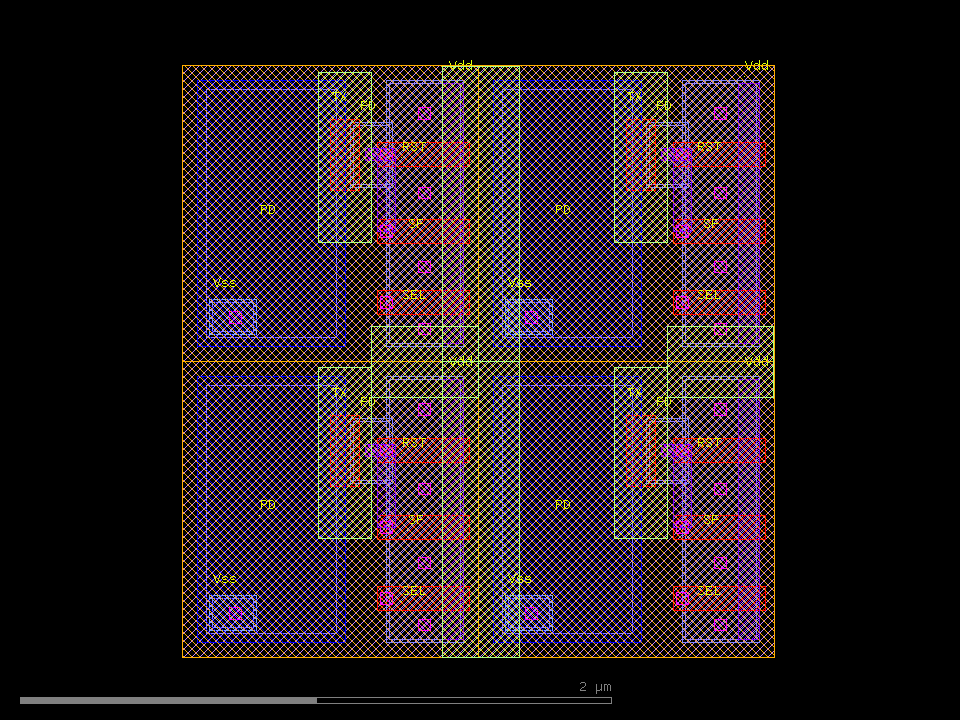
top_cell='CIS_APS', dbu=0.001 um, cells=2
bbox: (0,0;2,2) um
cells: ['APS_PIXEL', 'CIS_APS']

layer       shapes    area[um^2]   bbox[um]
2/0              4        4.0000   (0,0)-(2,2)
3/0             16        2.4192   (0.08,0.06)-(1.94,1.94)
4/0              8        1.0416   (0.57,0.05)-(1.95,1.95)
6/0             16        0.3936   (0.5,0.16)-(1.97,1.82)
9/0             12        0.3200   (0.62,0.06)-(1.95,1.94)
10/0             4        1.8000   (0.05,0.05)-(1.55,1.95)
Simple DRC
drc_check runs a list of rules against a file (path) or the current session and
reports, per rule, PASS/FAIL with violation counts and locations. Distances are in
micrometers; datatype defaults to 0.
Rule types
type |
Parameters | Meaning |
|---|---|---|
spacing |
layer, min |
Minimum space between shapes within one layer |
width |
layer, min |
Minimum feature width on a layer |
overlap |
layer, layer2 |
Forbidden overlap — any intersection of two layers is a violation |
separation |
layer, layer2, min |
Minimum space between two layers |
enclosure |
layer, layer2, min |
layer2 must surround layer by at least min |
Example
[
  {"type": "spacing",    "layer": 3, "datatype": 0, "min": 0.15},
  {"type": "width",      "layer": 6, "datatype": 0, "min": 0.08},
  {"type": "overlap",    "layer": 3, "layer2": 6},
  {"type": "separation", "layer": 3, "layer2": 10, "min": 0.05},
  {"type": "enclosure",  "layer": 3, "layer2": 10, "min": 0.02}
]
DRC: 5 rules, 3 failing
spacing 3/0 >= 0.15um: FAIL (8 violations)  at (0.550,0.692), (1.010,0.500), (1.820,1.000), (0.820,1.000)
width 6/0 >= 0.08um: PASS
forbidden overlap 3/0 & 6/0: FAIL (20 regions, 0.2784 um^2)  at (0.820,0.200), (1.820,0.200), (0.820,0.440), (1.820,0.440)
separation 3/0 <-> 10/0 >= 0.05um: FAIL (4 violations)  at (0.565,0.700), (1.565,0.700), (0.565,1.700), (1.565,1.700)
enclosure 10/0 of 3/0 >= 0.02um: PASS
max_report (default 10) caps the number of locations listed per rule.
Those locations can be drawn back as marker boxes to see exactly where the violations are. Here the OD spacing violations on the CIS pixel are highlighted on a marker layer:
Tip
The violation locations are centre points (in µm), so an assistant can read them
back, decide what to move, edit with the drawing tools, and re-run drc_check —
a closed correction loop.